
GPU vs CPU at Image Processing. Why GPU is much faster than CPU?I. INTRODUCTIONOver the past decade, there have been many technical advances in GPUs (graphics processing units), so they can successfully compete with established solutions (for example, CPUs, or central processing units) and be used for a wide range of tasks, including fast image processing. In this article, we will discuss the capabilities of GPUs and CPUs for performing fast image processing tasks. We will compare two processors and show the advantages of GPU over CPU, as well as explain why image processing on a GPU can be more efficient when compared to similar CPU-based solutions. In addition, we will go through some common misconceptions that prevent people from using a GPU for fast image processing tasks.
II. ABOUT FAST IMAGE PROCESSING ALGORITHMSFor the purposes of this article, we’ll focus specifically on fast image processing algorithms that have such characteristics as locality, parallelizability, and relative simplicity. Here’s a brief description of each characteristic:
Important criteria for fast image processingThe key criteria which are important for fast image processing are:
Maximum performance of fast image processing can be achieved in two ways: either by increasing hardware resources (specifically, the number of processors), or by optimizing the software code. When comparing the capabilities of GPU and CPU, GPU outperforms CPU in the price-to-performance ratio. It’s possible to realize the full potential of a GPU only with parallelization and thorough multilevel (both low-level and high-level) algorithm optimization.
Another important criterion is the image processing quality. There may be several algorithms used for exactly the same image processing operation that differ in resource intensity and the quality of the result. Multilevel optimization is especially important for resource-intensive algorithms and it gets essential performance benefits. After the multilevel optimization is applied, advanced algorithms will return results within a reasonable time period, comparable to the speed of fast but crude algorithms.
A GPU has an architecture that allows parallel pixel processing, which leads to a reduction in latency (the time it takes to process a single image). CPUs have rather modest latency, since parallelism in a CPU is implemented at the level of frames, tiles, or image lines. III. GPU vs CPU: KEY DIFFERENCESLet's have a look at the key differences between GPU and CPU. 1. The number of threads on a CPU and GPU CPU architecture is designed in such a way that each physical CPU core can execute two threads on two virtual cores. In this case, each thread executes the instructions independently. At the same time, the number of GPU threads is tens or hundreds of times greater, since these processors use the SIMT (single instruction, multiple threads) programming model. In this case, a group of threads (usually 32) executes the same instruction. Thus, a group of threads in a GPU can be considered as the equivalent of a CPU thread, or otherwise a genuine GPU thread. 2. Thread implementation on CPU and GPU One more difference between GPUs and CPUs is how they hide instruction latency. A CPU uses out-of-order execution for these purposes, whereas a GPU uses actual genuine thread rotation, launching instructions from different threads every time. The method used on the GPU is more efficient as a hardware implementation, but it requires the algorithm to be parallel and the load to be high. Thus it follows that many image processing algorithms are ideal for implementation on a GPU.
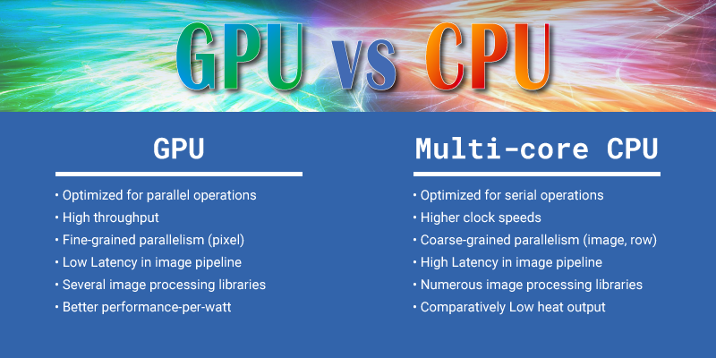
IV. ADVANTAGES OF GPU OVER CPU
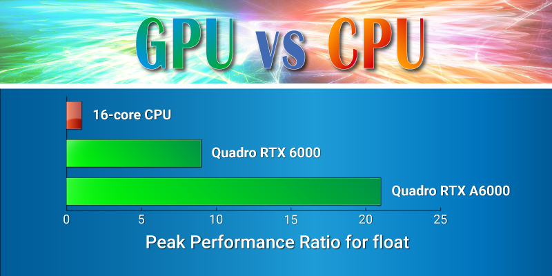
Still, all these advantages of a GPU over a CPU involve a high demand for parallelism of algorithms. While tens of threads are sufficient for maximum CPU load, tens of thousands are required to fully load a GPU. Embedded applicationsAnother type of task to consider is embedded solutions. In this case, GPUs are competing with specialized devices such as FPGAs (Field-Programmable Gate Arrays) and ASICs (Application-Specific Integrated Circuits). The main advantage of GPUs over these devices is significantly greater flexibility. A GPU is a serious alternative for some embedded applications, since powerful multi-core processors don’t meet requirements like size and power budget. V. USER MISCONCEPTIONS1. Users have no experience with GPUs, so they try to solve their problems with CPUs One of the main user misconceptions is associated with the fact that 10 years ago GPUs were considered inappropriate for high-performance tasks. But technologies are developing rapidly, and while GPU image processing integrates well with CPU processing, the best results are achieved when fast image processing is done on a GPU. 2. Multiple data copy to GPU and back kills performance This is another bias among users regarding GPU image processing. As it turns out, it’s a misconception as well, since in this case, the best solution is to implement all processing on the GPU within one task. The source data can be copied to the GPU just once, and the computation results are returned to the CPU at the end of the pipeline. In that case the intermediate data remains on the GPU. Copy can be also performed asynchronously, so it could be done in parallel with computations on the next/previous frame. 3. Small shared memory capacity, which is just 96 kB for each multiprocessor Despite the small capacity of GPU memory, the 96 KB memory size may be sufficient if shared memory is managed efficiently. This is the essence of software optimization for CUDA and OpenCL. It is not possible just to transfer software code from a CPU to a GPU without taking into consideration the specifics of the GPU architecture. 4. Insufficient size of the global GPU memory for complex tasks This is an essential point, which is first of all solved by manufacturers when they release new GPUs with a larger memory size. Second of all, it’s possible to implement a memory manager to reuse GPU global memory. 5. Libraries for processing on the CPU use parallel computing as well CPUs have the ability to work in parallel through vector instructions such as AVX or via multithreading (for example, via OpenMP). In most cases, parallelization occurs in the simplest way: each frame is processed in a separate thread, and the software code for processing one frame remains sequential. Using vector instructions involves the complexity of writing and maintaining code for different architectures, processor models, and systems. Vendor specific libraries like Intel IPP, are highly optimized. Issues arise when the required functionality is not in the vendor libraries and you have to use third-party open source or proprietary libraries, which can lack optimization. Another aspect which is negatively affecting the performance of mainstream libraries is the widespread adoption of cloud computing. In most cases, it’s much cheaper for a developer to purchase additional capacity in the cloud than to develop optimized libraries. Customers request quick product development, so developers are forced to use relatively simple solutions which aren’t the most effective. Modern industrial cameras generate video streams with extremely high data rates, which often preclude the possibility of transmitting data over the network to the cloud for processing, so local PCs are usually used to process the video stream from the camera. The computer used for processing should have the required performance and, more importantly, it must be purchased at the early stages of the project. Solution performance depends both on hardware and software. During the initial stages of the project, you should also consider what kind of hardware you’re using. If it’s possible to use mainstream hardware, any software can be used. If expensive hardware is to be used as a part of the solution, the price-performance ratio is rapidly increasing, and it requires using optimized software. Processing data from industrial video cameras involves a constant load. The load level is determined by the algorithms used and camera bitrate. The image processing system should be designed at the initial stages of the project in order to cope with the load within a guaranteed margin, otherwise it will be impossible to process the streams without data loss. This is a key difference from web systems, where the load is unbalanced. VI. SUMMARYSumming up, we come to the following conclusions: 1. GPU is an excellent alternative to CPU for solving complex image processing tasks. 2. The performance of optimized image processing solutions on a GPU is much higher than on a CPU. As a confirmation, we suggest that you refer to other articles on the Fastvideo blog, which describe other use cases and benchmarks on different GPUs for commonly used image processing and compression algorithms. 3. GPU architecture allows parallel processing of image pixels which, in turn, leads to a reduction of the processing time for a single image (latency). 4. High GPU performance software can reduce hardware cost in such systems, and high energy efficiency reduces power consumption. The cost of ownership of GPU-based image processing systems is lower than that of systems based on CPU only. 5. A GPU has the flexibility, high performance, and low power consumption required to compete with highly specialized FPGA / ASIC solutions for mobile and embedded applications. 6. Combining the capabilities of CUDA / OpenCL and hardware tensor kernels can significantly increase performance for tasks using neural networks. Addendum #1: Peak performance comparison for CPU and GPUWe will make the comparison for the float type (32-bit real value). This type suits well the most of image processing tasks. We will evaluate the performance per a single core. In the case of the CPU, everything is simple, we are talking about the performance of a single physical core. For the GPU, everything is somewhat more complicated. What is commonly called a GPU core is essentially an ALU, and according to NVIDIA terminology this is SP (Streaming Processor). The real analog of the CPU core is SM (this is Streaming Multiprocessor in NVIDIA terminology). The number of streaming processors in a single multiprocessor depends on the GPU architecture. For example, NVIDIA Turing graphics cards contain 64 SPs in one SM, while NVIDIA Ampere has 128 SPs. One SP can execute one FMA (Fused Multiply–Add) instruction per each clock cycle. The FMA instruction is selected here just for comparison, as it is used in convolution filters. Its integer counterpart is called MAD. The instruction (one of the variants) performs the following action: B = AX + B, where B is the accumulator that accumulates the convolution values, A is the filter coefficient, and X is the pixel value. By itself, such an instruction performs two operations: multiplication and summation. This gives us performance per clock cycle for SM: Turing - 2*64 = 128 FLOP, Ampere - 2*128 = 256 FLOP Modern CPUs have the ability to execute two FMA instructions from the AVX2 instruction set per each clock cycle. Each such instruction contains 8 float operands and 16 FLOP operations, respectively. In total, one CPU core performs 2*16 = 32 FLOP per clock cycle. To get performance per unit of time, we need to multiply the number of instructions per clock cycle by the frequency of the device. On average, the GPU frequency is in the range of 1.5 - 1.9 GHz, and the CPU with a load on all cores has a frequency around 3.5 – 4.5 GHz. The FMA instruction from the AVX2 set is quite heavy for the CPU. When they are performed, a large part of CPU is involved, and heat generation increases greatly. This causes the CPU to lower the frequency to avoid overheating. For different CPU series, the amount of frequency reduction is different. For example, according to this article, we can estimate a decrease to the level of 0.7 from the maximum. Next, we will take the coefficient 0.8, it corresponds to newer generations of CPUs. We can assume that the CPU frequency is 2.5 times higher than that of the GPU. Taking into account the frequency reduction factor when working with AVX2 instructions, we get 2.5*0.8 = 2. In total, the relative performance in FLOP for the FMA instruction when compared with the CPU core is the following: Turing SM = 128 / (2.0*32) = 2 and for Ampere SM it is 256 / (2.0*32) = 4 times, i.e. one SM is more powerful than one CPU core. Let's estimate the performance of L1 for the CPU core. Modern CPUs can load two 256-bit registers from the L1 cache in parallel or 64 bytes per clock cycle. The GPU has a unified shared memory/L1 block. The shared memory performance is the same both for Turing and Ampere architectures, and is equal to 32 float values per clock cycle, or 128 bytes per clock cycle. Taking into account the frequency ratio, we get a performance ratio of 128 (bytes per clock) / (2 (CPU frequency is greater than GPU) * 64 (bytes per clock)) = 1. Also compare the L1 and shared memory sizes for CPU and GPU. For the CPU, the standard size of the L1 data cache is 32 kB. Turing SM has 96 kBytes of unified shared memory/L1 (shared memory takes 64 kBytes), and Ampere SM has 128 kBytes of unified shared memory/L1 (shared memory takes 100 kBytes). To evaluate the overall performance, we need to calculate the number of cores per one device or socket. For desktop CPUs, we consider the option of 16 cores (AMD Ryzen, Intel i9). It could be considered as average core number for high performance CPUs on the market. NVIDIA Quadro RTX 6000 with Turing architecture has 72 SMs. NVIDIA Quadro RTX A6000 which is based on Ampere architecture has 84 SMs. The total ratio of the number of GPU SMs to CPU cores are 72/16 = 4.5 (Turing) and 84/16 = 5.25 (Ampere). Based on this, we can evaluate the overall performance for the float type. For top Turing graphics cards, we get: 4.5 (the ratio of the number of GPU/CPU cores) * 2 (the ratio of single SM performance to the performance of one CPU core) = 9 times. Let's estimate the relative throughput of CPU L1 and GPU shared memory. We get 4.5 (the ratio of the number of GPU/CPU cores) * 1 (the ratio of single SM throughput to the one of single CPU core) = 4.5 times for Turing, and 5.25 * 1 = 5.25 for Ampere respectively. The ratios can vary slightly for a specific CPU model, but an order of magnitude will be the same.
We've obtained the result that reflects a significant advantage of the GPU over the CPU in both performance and on-chip memory throughput in computations, which are related to image processing. It is very important to bear in mind that these results are obtained for the CPU only in the case of using AVX2 instructions. In the case of using scalar instructions, the CPU performance is reduced by 8 times, both in arithmetic operations and in the memory throughput. Therefore, for modern CPUs, software optimization is of particular importance. Let's say a few words about the new AVX-512 instruction set for the CPU. This is the next generation of SIMD instructions with a vector length increased to 512 bits. Performance is expected to double in the future compared to AVX2. Modern versions of the CPU provide a speedup of up to 1.6 times, as they require even more frequency reduction than the instructions from the AVX2. The AVX-512 has not yet been widely distributed in the mass segment, but this is likely to happen in the future. The disadvantages of this approach will be the need to adapt the algorithms to a new vector length and recompile the code for support. Let's try to compare the system memory bandwidth. Here we can see a significant spread of values. For the CPU, the initial numbers are 50 GB/s (2-channel DDR4 3200 controller) for mass-market CPUs. In the workstation segment the CPUs with four-channel controllers dominate with a bandwidth around 100 GB/s. For servers we can see CPUs with 6-8 channel controllers and a performance could be more than 150 GB/s. For the GPU, the value of global memory bandwidth could vary in a wide range. It starts from 450 GB/s for the Quadro RTX 5000 and it could reach 1550 GB/s for the latest A100. As a result, we can say that the throughputs in comparable segments differ significantly, the difference could be up to an order of magnitude. From all of the above, we can conclude that the GPU is significantly (sometimes almost by an order of magnitude) superior to the CPU that executes optimized code. In the case of non-optimized code for the CPU, the difference in performance can be even greater, up to 50-100 times. All this creates serious prerequisites for increasing productivity in widespread image processing applications.
Addendum #2 - memory-bound and compute bound algorithmsWhen we are talking about these types of algorithms, it is important to understand that we imply a specific implementation of the algorithm on a specific architecture. Each processor has some peak arithmetic performance. If the implementation of the algorithm can reach the peak performance of the processor on the target instructions, then it is compute-bound, otherwise the main limitation will be memory access and the implementation becomes memory-bound. The memory subsystem of all processors is hierarchical, consisting of several levels. The closer the level is to the processor, the smaller it is in volume and the faster it is. The first level is the L1 data cache, and at the last level is the RAM or the global memory. The algorithm can initially be compute-bound at the first level of the hierarchy, and then to become memory-bound at higher levels of the hierarchy. We could consider a task to sum two arrays and to write the result to the third one. You can write this as X = Y + Z, where X, Y, Z are arrays. Let's say we use the AVX instructions to implement the solution on the processor. Then we will need two reads, one summation, and one write per element. A modern CPU can perform two reads and one write simultaneously to the L1 cache. But at the same time, it can also execute two arithmetic instructions, and we can only use just one. This means that the array summation algorithm is memory-bound at the first level of the memory hierarchy. Let's consider the second algorithm, which is image filtering in a 3×3 window. Image filtering is based on the operation of convolution of the pixel neighborhood with filter coefficients. The MAD (or FMA, depending on the architecture) instruction is used to calculate the convolution. For window 3×3 we need 9 of these instructions. We actually need to do the following: B = AX + B, where B is the accumulator to store the convolution values, A is the filter coefficient, and X is the pixel value. The values of A and B are in registers, and the pixel values are loaded from memory. In this case, one load is required per FMA instruction. Here, the CPU is able to supply two FMA ports with data due to two loads, and the processor will be fully loaded. The algorithm can be considered compute-bound. Let's look at the same algorithm at the RAM access level. We can take the most memory-efficient implementation, when a single reading of a pixel updates all 9 the windows it belongs. In this case, there are 9 FMA instructions per read operation. Thus, a single CPU core processing float data at 4 GHz requires 2 (instructions per clock cycle) × 8 (float in AVX register) × 4 (Bytes in float) × 4 (GHz) / 9 = 28.5 GB/s. The dual-channel controller with DDR4-3200 has a peak throughput of 50 GB/s and could serve as a data source just for two CPU cores in this task. Therefore, such an algorithm running on an 8-16 core processor is memory-bound. This is despite the fact that at the lower level it is balanced. Now we consider the same algorithm when implemented on the GPU. It is immediately clear that the GPU has a less balanced architecture at the SM level with a bias to computing. For the Turing architecture, the ratio of the speed of arithmetic operations (in float) to the load throughput from shared memory is 2:1, for the Ampere architecture this is 4:1. Due to the larger number of registers on the GPU, you can implement the above optimization on the GPU registers. This allows us to balance the algorithm even for Ampere. And at the shared memory level, the implementation remains compute-bound. From the point of view of the top level memory (global memory), the calculation for the Quadro RTX 5000 (Turing) gives the following results: 64 (operations per clock cycle) × 4 (Bytes in float) × 1.7 (GHz) / 9 = 48.3 GB/s per SM. The ratio of total throughput to SM throughput is 450 / 48.3 = 9.3 times. The total number of SMs in the Quadro RTX 5000 is 48. That is, for the GPU, the high-level filtering algorithm is memory-bound. As the window size grows, the algorithm becomes more complex and shifts towards compute-bound accordingly. Most image processing algorithms are memory-bound at the global memory level. And since the global memory bandwidth of the GPU is in many cases an order of magnitude greater than that of the CPU, this provides a comparable performance gain.
Addendum #3: SIMD and SIMT models, or why there are so many threads on GPUTo improve CPU performance, SIMD (single instruction, multiple data) instructions are used. One such instruction allows us to perform several similar operations on a data vector. The advantage of this approach is that it increases performance without significantly modifying the instruction pipeline. All modern CPUs, both x86 and ARM, have SIMD instructions. The disadvantage of this approach is the complexity of programming. The main approach to SIMD programming is to use intrinsic. Intrinsic are built-in compiler functions that contain one or more SIMD instructions, plus instructions for preparing parameters. Intrinsic forms a low-level language very close to assembler, which is extremely difficult to use. In addition, for each instruction set, each compiler has its own Intrinsic set. As soon as a new set of instructions comes out, we need to rewrite everything. If we switch to a new platform (from x86 to ARM) you need to rewrite all the software. If we start using another compiler - again, we need to rewrite the software. The software model for the GPU is called SIMT (Single instruction, multiple threads). A single instruction is executed synchronously in multiple threads. This approach can be considered as a further development of SIMD. The scalar software model hides the vector essence of the hardware, automating and simplifying many operations. That is why it is easier for most software engineers to write the usual scalar code in SIMT than vector code in pure SIMD. CPU and GPU have different ways to solve the issue of instruction latency when executing them on the pipeline. The instruction latency is how many clock cycles the next instruction wait for the result of the previous one. For example, if the latency of an instruction is 3 and the CPU can run 4 such instructions per clock cycle, then in 3 clock cycles the processor can run 2 dependent instructions or 12 independent ones. To avoid pipeline stalling, all modern processors use out-of-order execution. In this case, the processor analyzes data dependencies between instructions in out-of-order window and runs independent instructions out of the program order. The GPU uses a different approach which is based on multithreading. The GPU has a pool of threads. Each clock cycle, one thread is selected and one instruction is chosen from that thread, then that instruction is sent for execution. On the next clock cycle, the next thread is selected, and so on. After one instruction has been run from all the threads in the pool, GPU returns to the first thread, and so on. This approach allows us to hide the latency of dependent instructions by executing instructions from other threads. When programming the GPU, we have to distinguish two levels of threads. The first level of threads is responsible for SIMT generation. For the NVIDIA GPU, these are 32 adjacent threads, which are called warp. SM for Turing is known to support 1024 threads. This number is divided into 32 real threads, within which SIMT execution is organized. Real threads can execute different instructions at the same time, unlike SIMT. Thus, the Turing streaming multiprocessor is a vector machine with a vector size of 32 and 32 independent real threads. The CPU core with AVX is a vector machine with a vector size of 8 and two independent threads. |